BROWSE
Detail
Registered METHOD OF FABRICATING PSEUDOMORPHIC HIGH ELECTRON MOBILITY TRANSISTOR
- Inventors
- Jong-Won Lim, Hae Cheon Kim, Hokyun Ahn, Woojin Chang, Ji Hong Gu, Mun Jae Kyoung
- Application No.
- 11446750 (2006.06.05)
- Publication No.
- 20070134862 (2007.06.14)
- Registration No.
- 7419862 (2008.09.02)
- Country
- UNITED STATES
- Project Code
- 05MB1400, SoP(System on Package) for 60 GHz Pico cell Communication, Cho Kyoung Ik
- Abstract
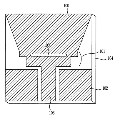
- Provided is a method of fabricating a pseudomorphic high electron mobility transistor (PHEMT). The method includes the steps of: preparing a substrate including a channel layer and a capping layer that is the uppermost layer; forming a source and a drain on the capping layer; forming a first protective layer on the entire surface of the resultant structure and then patterning the first protective layer to expose a portion of the capping layer in a channel region; removing the exposed portion of the capping layer to form a first recess structure; forming a second protective layer on the entire surface of the resultant structure and then patterning the second protective layer to expose a portion of the substrate in the first recess structure so that a second recess structure is formed; forming a multilayered photoresist layer on the entire surface of the resultant structure and then patterning the multilayered photoresist layer to expose a portion of the substrate through the second recess structure and form a gate-shaped opening; and depositing a metal layer to fill the gate-shaped opening and then removing the multilayered photoresist layer to form a gate connected to the substrate through the second recess structure.
- KSP Keywords
- Capping layer, Channel layer, High electron, High electron mobility, High-electron mobility transistor(HEMT), Protective layer, electron mobility, metal layer, pseudomorphic high electron mobility transistor(pHEMT), recess structure